Advanced Packaging Has Become the Bottleneck
Intel (INTC) is attempting to reposition itself in the semiconductor value chain by leveraging one of the few areas where it still holds a differentiated capability—advanced packaging. While Taiwan Semiconductor Manufacturing Company’s (TSM) (TSMC) Chip on Wafer on Substrate (CoWoS) platform has become the industry standard for high-performance AI processors, Intel is now promoting its Embedded Multi-die Interconnect Bridge-T (EMIB-T) as a viable alternative in a market increasingly constrained by capacity rather than technology.
In 2026, semiconductor growth is not being driven by PCs or smartphones, largely because of the shortage and concomitant high price of commodity DRAMs. Instead, it is driven by hyperscaler capital expenditures that are tied to artificial intelligence infrastructure. That demand is running directly into a packaging bottleneck rather than a wafer fabrication bottleneck.
In Chart 1, I show my analysis of CoWoS demand, which I forecast will grow at a 64% CAGR between 2025 and 2027. This growth is driven primarily by the rapid increase in AI accelerator complexity and the corresponding growth in HBM content per processor. Indeed, Nvidia’s (NVDA) move to 1-year cadence of new and more powerful GPU ships demanding more memory, has been a strong catalyst in altering the supply/demand dynamics of the memory industry.
My analysis indicates that this demand growth is concentrated among Nvidia, Advanced Micro Devices (AMD), Broadcom (AVGO), and hyperscaler Application Specific Integrated Circuits (ASIC) programs. Together they absorb most leading-edge CoWoS capacity. Unlike prior semiconductor cycles what were driven by broad consumer demand, this growth is concentrated and constrained by packaging availability rather than wafer fabrication capacity.
With Nvidia and hyperscalers consuming most available CoWoS capacity, smaller AI chip developers are forced to look for alternative packaging solutions, creating an opportunity for Intel’s Embedded Multi-die Interconnect Bridge (EMIB).
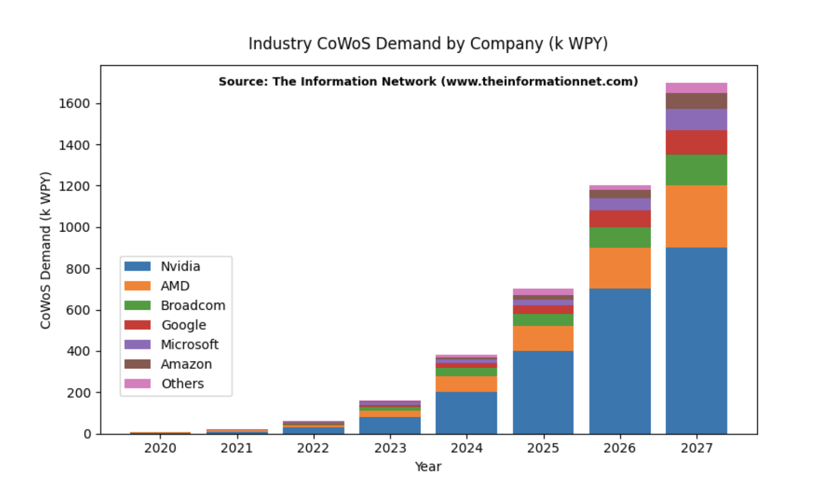
Chart 1
CoWoS remains the dominant solution for high-end AI accelerators because of its ability to integrate GPUs with high-bandwidth memory using a silicon interposer. This architecture enables extremely high interconnect density and memory bandwidth measured in terabytes per second, making it indispensable for training large language models.
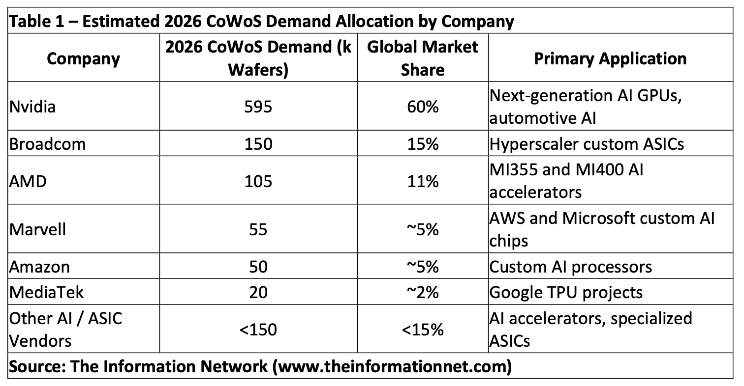
However, that dominance has created a structural imbalance, as CoWoS capacity is effectively pre-allocated to a small number of customers, led by Nvidia, which is estimated to account for roughly 60% of total demand. Broadcom, AMD, and hyperscaler ASIC programs absorb most of the remaining capacity, leaving limited availability for second-tier AI chip developers.
According to Table 1 and illustrated in Chart 1, Nvidia alone is expected to account for 60% of global CoWoS demand in 2026, while Broadcom and AMD absorb another 26%. This results in limited capacity available for smaller AI chip developers and custom ASIC vendors and the need for an alternate supplier to TSMC. Data for this analysis comes from my report entitled “High-Density Semiconductor Packaging : Market Analysis and Technology Trends,” which can be previewed at my web site The Information Network.
Intel’s EMIB-T: A Cost and Scale Alternative
Intel’s EMIB technology, originally developed for internal products such as its Xeon and GPU platforms, is now being offered externally through Intel Foundry Services. EMIB-T represents an evolution of this architecture, embedding silicon bridges and through-silicon vias directly into the substrate rather than relying on a full silicon interposer.
Chart 2 compares the two packaging structures. CoWoS uses a full silicon interposer connecting logic and HBM across the entire package, while EMIB uses localized silicon bridges embedded within the substrate, thereby reducing silicon area and lowering package cost.
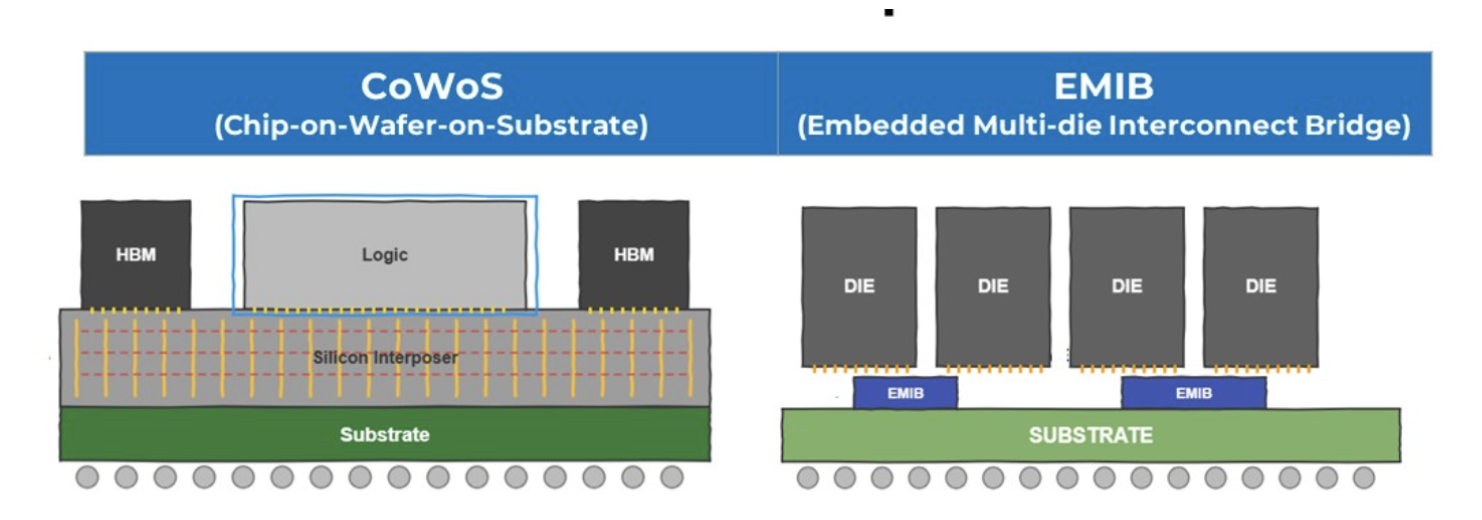
Chart 2
The distinction between EMIB and CoWoS is not simply architectural but economic.
According to Table 2, CoWoS and EMIB target different portions of the AI market. CoWoS remains the preferred solution for maximum bandwidth and high-end AI training processors, while EMIB focuses on lower-cost, large-package designs for ASICs and inference accelerators.
According to my analysis in previous articles, inference ASICs with HBM represented approximately 20% of total HBM processor demand in 2025, but that percentage is expected to increase to 36% by 2027 as hyperscalers increasingly deploy custom inference accelerators alongside traditional AI training GPUs.
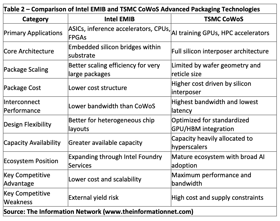
Based on industry packaging economics, EMIB offers a significantly lower package cost than CoWoS, which can approach $1,000 per Rubin-class processor due to the large silicon interposer.
This advantage becomes more pronounced as AI processors continue to scale in size and complexity. Current CoWoS implementations support package sizes of roughly 3.3 times reticle size. Future generations of CoWoS (illustrated in Chart 3 below) are expected to extend to 5.5 times and eventually 9.5 times by 2027. Intel, by contrast, has stated that EMIB supported approximately 6 times reticle size in 2024 and is targeting 8 times in 2026 and as much as 12 times by 2028.
Capacity Constraints Define the Opportunity
As I noted above, Intel’s opportunity is driven as much by available packaging capacity as by technology. While TSMC continues to expand CoWoS capacity aggressively, demand continues to exceed supply due to the rapid growth of AI infrastructure.
TSMC is targeting CoWoS capacity of approximately 130,000 to 160,000 wafers per month by 2026–2027. Yet demand from Nvidia, Broadcom, AMD, and hyperscalers absorbs most of this output.
TSMC’s Arizona Fab 21 complex gives the company a growing U.S. manufacturing footprint as well, although most CoWoS capacity remains concentrated in Taiwan. Intel already operates advanced packaging facilities in New Mexico and Malaysia and is expanding packaging capacity in Arizona alongside its Fab 52 and Fab 62 buildout.
As AI customers increasingly seek geographic diversification of the supply chain, domestic advanced packaging capability is becoming strategically important.
These expansions in capacity and manufacturing enable the companies to expand technology complexity. According to Chart 3, the advanced packaging market is evolving into a competitive ecosystem spanning 2.5D and 3D integration technologies, with TSMC, Intel, and Samsung each developing differentiated architectures targeting AI, HPC, and heterogeneous integration.
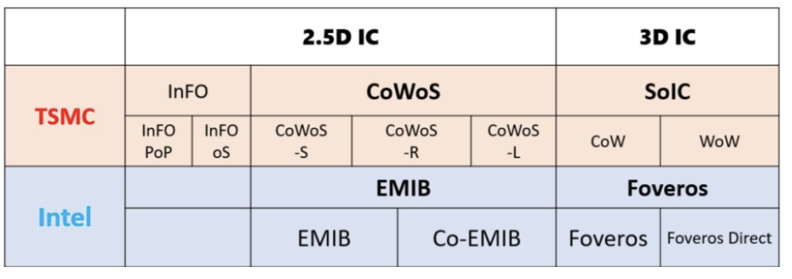
Chart 3
There are early indications that this strategy is gaining traction. Industry reports indicate that a Google–MediaTek collaboration is evaluating EMIB-T for a 2027 tensor processing unit, while Meta is considering the technology for its MTIA accelerators.
Execution Risk Remains the Key Variable
Despite these advantages, Intel faces significant challenges in scaling EMIB-T as a commercial offering. Unlike CoWoS, which has a well-established production track record, EMIB-T has yet to demonstrate consistent high-volume yields in external manufacturing.
In advanced packaging, yield determines cost. Why, because a failed package results in the loss of high-value logic dies and multiple stacks of high-bandwidth memory, meaning that EMIB’s cost advantage depends entirely on achieving competitive yields at scale. I discussed that issue in my May 4, 2026 247 Wall St. article entitled “KLA Is Gaining Share as AI Chip Complexity Drives Up Yield Costs.”
From a financial perspective, the near-term impact is incremental rather than transformative.
Investor Takeaway
Intel’s EMIB-T is not a direct replacement for TSMC’s CoWoS, as the two technologies are optimized for different segments of the AI market. CoWoS will remain the dominant solution for high-end training processors where maximum bandwidth and performance are required.
However, the AI market is expanding beyond training into inference, custom silicon, and cost-optimized deployments, where the constraints of CoWoS—cost, capacity, and availability—become more relevant.
According to Chart 1 above, the defining feature of the current semiconductor cycle is not uncertain demand but constrained supply. At the advanced packaging level, this constrained supply from TSMC creates a secondary market opportunity for alternative technologies such as EMIB-T.
Intel’s opportunity lies in addressing this gap, and if EMIB-T can achieve competitive yields and scale, it can serve as a second source for AI packaging, particularly for ASICs and inference accelerators.
Intel does not need to displace CoWoS to benefit from AI growth. It only needs to capture a portion of incremental packaging demand in a market where supply remains constrained.
In this cycle, competitive positioning is determined not only by chip performance but by access to packaging capacity. Even a secondary position in a supply-constrained market can translate into meaningful revenue growth and improved strategic relevance for Intel.